China-US team’s feat could ‘open entirely new avenues’ in semiconductors
AI Summary
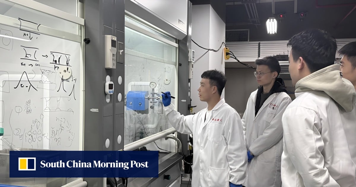
A joint Chinese-US research team has developed a new semiconductor manufacturing method that could revolutionize the development of high-performance light-emitting and integrated devices. The team's "self-etching" technique allows for the creation of intricate structures in superthin lead halide perovskites, a promising semiconductor material, without causing damage. This is significant because conventional lithography, the current standard, struggles with these soft and unstable materials due to uncontrolled damage from sideways light. The new process enables controlled lateral microstructures, adding a new dimension to semiconductor design. This breakthrough could surpass the limitations of current lithography and open new avenues for semiconductor performance improvements.
Key Entities & Roles
Keywords
Sentiment Analysis
Source Transparency
This article was automatically classified using rule-based analysis.
Topic Connections
Explore how the topics in this article connect to other news stories
Find Similar Articles
AI-PoweredDiscover articles with similar content using semantic similarity analysis.