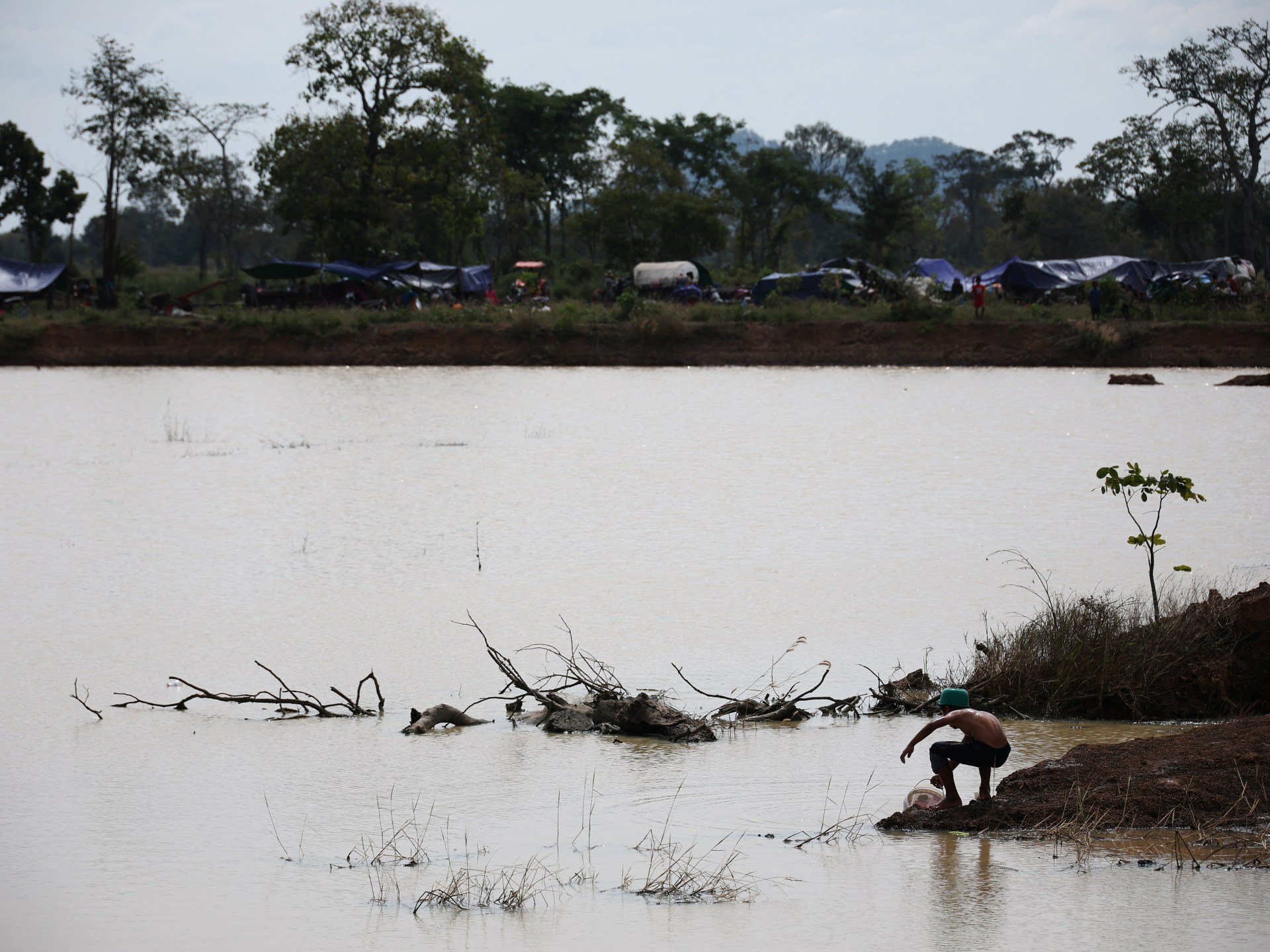
US offers to mediate more talks to end the latest flare-up of violence, which has upended an October peace accord.Published On 26 Dec 2025Cambodia has accused Thai forces of carrying out “ruthless” aerial attacks against it, even as the two sides hold new talks aimed at easing their long-running border conflict.Thai fighter jets dropped dozens of bombs near the northwestern Cambodian village of Chouk Chey early on Friday morning, causing “extensive destruction to civilians’ homes, properties, and public infrastructure”, Cambodia’s state news agency cited the defence ministry as saying.Recommended Stories list of 3 itemslist 1 of 3Video: What’s behind Thailand and Cambodia’s border dispute?list 2 of 3Cambodia says Thailand bombed casino hub on border, with no truce in sightlist 3 of 3Ukraine accepts demilitarised zone to end Russia war, but do DMZs work?end of listLater in the morning, Thai forces also launched artillery attacks in the Stung Bot area near the border, reported the Cambodian news agency Agence Kampuchea Presse.Cambodia’s defence ministry condemned the attacks as “grave acts of aggression” that intentionally endangered “civilian lives and civilian infrastructure”. It said the attacks in Chouk Chey were “exceptionally ruthless and inhumane”.The violence marks the latest flare-up since renewed clashes broke out on December 8, derailing an expanded ceasefire brokered by the United States and Malaysia in October. Fighting this month has killed at least 96 people, according to authorities on both sides, while displacing about one million people.Defence officials from Thailand and Cambodia held their first talks since renewed clashes started, on Wednesday, though they did not appear to produce any major diplomatic breakthrough.Cambodia’s Defence Ministry spokesperson Maly Socheata said the two sides planned to continue further talks under a bilateral border committee on Friday, according to the Anadolu news agency.
SRCAl Jazeera
LANGEN
LEANCenter
WORDS290
FRI · 2025-12-26 · 07:33 GMTBRIEF NSR-2025-1226-4328
NSR-2025-1226-4328News Report·EN·Conflict
Cambodia blames Thailand for ‘ruthless’ bombardment amid border talks
On December 26, 2025, Cambodia accused Thailand of "ruthless" aerial and artillery attacks near the village of Chouk Chey and the Stung Bot area, causing damage to civilian infrastructure. These attacks occurred despite ongoing talks aimed at resolving the long-running border conflict.
Stephen QuillenAl JazeeraFiled 2025-12-26 · 07:33 GMTLean · CenterRead · 2 min
Al JazeeraFIG 01
Reading time
2min
Word count
290words
Sources cited
4cited
Entities identified
0entities
Quality score
75%
§ 01
Briefing Summary
AI-generatedNEWSAR · AI
On December 26, 2025, Cambodia accused Thailand of "ruthless" aerial and artillery attacks near the village of Chouk Chey and the Stung Bot area, causing damage to civilian infrastructure. These attacks occurred despite ongoing talks aimed at resolving the long-running border conflict. Cambodia's defense ministry condemned the actions as grave aggression endangering civilian lives. The violence is a recent escalation since renewed clashes began on December 8, disrupting a ceasefire brokered in October. The fighting has resulted in at least 96 deaths and displaced approximately one million people. While defense officials from both countries have engaged in talks, no major diplomatic breakthroughs have been achieved.
Confidence 0.90Sources 4Claims 5
§ 02
Article analysis
Model · rule-basedFraming
Conflict
Diplomatic
Tone
Mixed Tone
AI-assessed
CalmNeutralAlarmist
Factuality
0.80 / 1.00
Factual
LowHigh
Sources cited
4
Well sourced
FewMany
§ 03
Key claims
5 extracted01
Defence officials from Thailand and Cambodia held their first talks since renewed clashes started, on Wednesday.
factual
Confidence
1.00
02
Violence marks the latest flare-up since renewed clashes broke out on December 8.
factual
Confidence
1.00
03
Fighting this month has killed at least 96 people.
statisticauthorities on both sides
Confidence
1.00
04
Thai fighter jets dropped dozens of bombs near the northwestern Cambodian village of Chouk Chey.
factualCambodia’s state news agency
Confidence
1.00
05
Cambodia has accused Thai forces of carrying out “ruthless” aerial attacks.
quoteCambodia's state news agency
Confidence
1.00
§ 04
Full report
2 min read · 290 words§ 06
Keywords & salience
9 termsborder conflict
0.90
aerial attacks
0.80
cambodia
0.80
thailand
0.80
border talks
0.70
civilian infrastructure
0.60
ceasefire
0.50
military aggression
0.50
displaced people
0.40
§ 07
Topic connections
Interactive graph No topic relationship data available yet. This graph will appear once topic relationships have been computed.