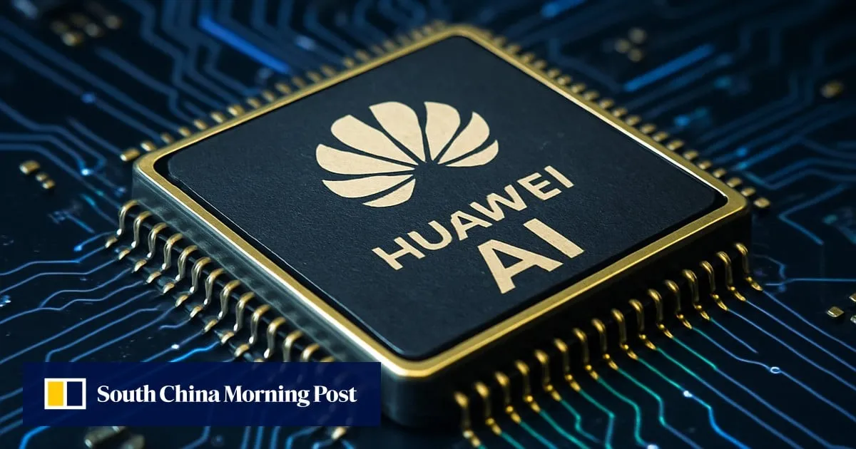
Huawei Technologies has unveiled a new scaling law and chip architecture intended to deliver transistor performance equivalent to a 1.4-nanometre process node – representing the leading edge of semiconductor development – in a few years without relying on advances in lithography tools.The move represents a significant step by the Chinese tech giant to establish a self-reliant semiconductor ecosystem.The company claims the new Tau (τ) Scaling Law, which was presented on Monday by He Tingbo, chairwoman of the Huawei Scientist Committee and president of the company’s semiconductor business department, is a new principle guiding “evolution of both semiconductors and electronic systems”.
SRCSouth China Morning Post
LANGEN
LEANCenter-Right
WORDS100
ENT9
MON · 2026-05-25 · 01:30 GMTBRIEF NSR-2026-0525-79051
NSR-2026-0525-79051News Report·EN·Technology
Huawei unveils new scaling law and tech that narrows gap with TSMC, Samsung
Huawei Technologies has introduced a new scaling law and chip architecture designed to achieve transistor performance comparable to a 1.4-nanometre process node. This development aims to advance semiconductor technology without depending on improvements in lithography tools.
Ann Cao,Iris DengSouth China Morning PostFiled 2026-05-25 · 01:30 GMTLean · Center-RightRead · 1 min
South China Morning PostFIG 01
Reading time
1min
Word count
100words
Sources cited
1cited
Entities identified
9entities
Quality score
100%
§ 01
Briefing Summary
AI-generatedNEWSAR · AI
Huawei Technologies has introduced a new scaling law and chip architecture designed to achieve transistor performance comparable to a 1.4-nanometre process node. This development aims to advance semiconductor technology without depending on improvements in lithography tools. The company presented the new Tau (τ) Scaling Law on Monday, with He Tingbo, chairwoman of the Huawei Scientist Committee and president of the company’s semiconductor business department, explaining it as a guiding principle for the evolution of semiconductors and electronic systems. This initiative marks a significant effort by Huawei to build a self-reliant semiconductor ecosystem.
Confidence 0.85Sources 1Claims 4Entities 9
§ 02
Article analysis
Model · rule-basedFraming
Technology
Economic Impact
Tone
Measured
AI-assessed
CalmNeutralAlarmist
Factuality
0.70 / 1.00
Factual
LowHigh
Sources cited
1
Limited
FewMany
§ 03
Key claims
4 extracted01
Huawei claims its new Tau (τ) Scaling Law is a new principle guiding the evolution of semiconductors and electronic systems.
quoteHe Tingbo (Huawei)
Confidence
0.95
02
Huawei unveiled a new scaling law and chip architecture aiming for transistor performance equivalent to a 1.4nm process node.
factualHuawei Technologies
Confidence
0.90
03
The move signifies Huawei's effort to establish a self-reliant semiconductor ecosystem.
factualHuawei Technologies
Confidence
0.90
04
The new technology aims to achieve leading-edge semiconductor development without relying on advances in lithography tools.
factualHuawei Technologies
Confidence
0.80
§ 04
Full report
1 min read · 100 words§ 05
Entities
9 identifiedKey playerOppositionContextPositiveNeutralNegative
Organizations4
Locations1
§ 06
Keywords & salience
9 termsscaling law
1.00
semiconductor ecosystem
1.00
huawei
0.90
chip architecture
0.80
transistor performance
0.70
lithography tools
0.60
tsmc
0.50
samsung
0.50
1.4-nanometre process node
0.50
§ 07
Topic connections
Interactive graph Network visualization showing 21 related topics
View Full Graph Person Organization Location Event|Click node to navigate|Edge numbers = shared articles