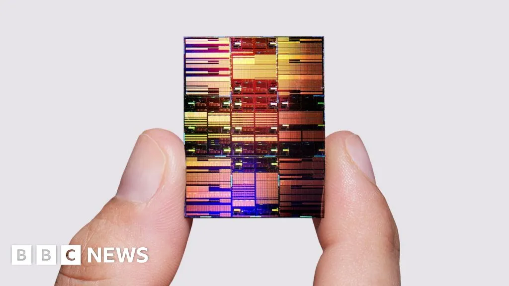
IBM has unveiled a new chip design which it says could enable manufacturers to cram 100 billion transistors on a silicon chip the size of a fingernail.The current industry-standard size for chips, measured in a the unit of nanometres - a billionth of a metre and the size of a few atoms - is around two nanometres (nm). But IBM claims its new chip tech is the equivalent of around 0.7nm, which may make it the world's first known chip technology below 1nm. However, it will be several years before the chip tech could be ready to go into production.The firm claims in tests, its prototype performed 50% better than its own 2nm chip and was 70% more energy efficient.It claimed similar boosts in performance when it debuted its 2nm chip tech back in 2021 - saying at the time its tests of those, slightly larger, chips produced similar leaps in performance and energy efficiency.Jay Gambetta, director of IBM Research and IBM Fellow, described the NanoStack tech as a "landmark moment" for the future of chips."With our new NanoStack architecture, we're not just making smaller transistors, we're reinventing how chips are built to deliver dramatically more power and energy efficiency," he said.
SRCBBC News - World
LANGEN
LEANCenter
WORDS202
ENT6
THU · 2026-06-25 · 10:04 GMTBRIEF NSR-2026-0625-87327
NSR-2026-0625-87327News Report·EN·Technology
IBM hails new 'block of flats' design breakthrough for ultra tiny chips
IBM has announced a breakthrough in chip technology, developing a design that could enable chips to hold 100 billion transistors on a fingernail-sized surface. This new technology is reportedly equivalent to around 0.7 nanometers, placing it below the current industry standard of two nanometers.
2 hours agoShareSaveAdd as preferred on GoogleZoe KleinmanTechnology editorBBC News - WorldFiled 2026-06-25 · 10:04 GMTLean · CenterRead · 1 min
BBC News - WorldFIG 01
Reading time
1min
Word count
202words
Sources cited
1cited
Entities identified
6entities
Quality score
100%
§ 01
Briefing Summary
AI-generatedNEWSAR · AI
IBM has announced a breakthrough in chip technology, developing a design that could enable chips to hold 100 billion transistors on a fingernail-sized surface. This new technology is reportedly equivalent to around 0.7 nanometers, placing it below the current industry standard of two nanometers. In tests, this prototype demonstrated a 50% performance improvement and 70% greater energy efficiency compared to IBM's own 2nm chips. While this represents a significant advancement, IBM states that the technology is still several years away from being ready for production. The company describes this new NanoStack architecture as a "landmark moment" for future chip development, aiming to deliver increased power and energy efficiency by fundamentally changing how chips are constructed.
Confidence 0.90Sources 1Claims 5Entities 6
§ 02
Article analysis
Model · rule-basedFraming
Technology
Economic Impact
Tone
Mixed Tone
AI-assessed
CalmNeutralAlarmist
Factuality
0.70 / 1.00
Factual
LowHigh
Sources cited
1
Limited
FewMany
§ 03
Key claims
5 extracted01
The NanoStack tech is a 'landmark moment' for the future of chips.
quoteJay Gambetta
Confidence
0.95
02
It will be several years before the chip tech could be ready to go into production.
prediction
Confidence
0.90
03
IBM has unveiled a new chip design that could enable manufacturers to cram 100 billion transistors on a silicon chip the size of a fingernail.
factualIBM
Confidence
0.90
04
IBM's new chip tech is the equivalent of around 0.7nm, potentially making it the world's first chip technology below 1nm.
factualIBM
Confidence
0.85
05
In tests, its prototype performed 50% better than its own 2nm chip and was 70% more energy efficient.
statisticIBM
Confidence
0.80
§ 04
Full report
1 min read · 202 words§ 05
Entities
6 identifiedKey playerOppositionContextPositiveNeutralNegative
Organizations1
§ 06
Keywords & salience
9 termschip design
1.00
tiny chips
0.90
transistors
0.80
nanometres
0.70
nanostack
0.60
ibm
0.60
performance
0.50
energy efficiency
0.50
silicon chip
0.40
§ 07
Topic connections
Interactive graph No topic relationship data available yet. This graph will appear once topic relationships have been computed.